(China (Mainland))


Product Summary
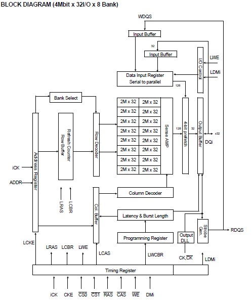
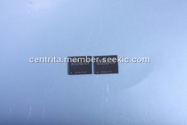
The K4J10324QD-HC14 is 1G bits of hyper synchronous data rate Dynamic RAM organized as 16 x 2,097,152 words by 32 bits, fabricated with SAMSUNGs high performance CMOS technology. Synchronous features with Data Strobe allow extremely high performance up to 8.0GB/s/chip. I/O transactions are possible on both edges of the clock cycle. Range of operating frequencies, and programmable latencies allow the device to be useful for a variety of high performance memory system applications.
Parametrics
Absolute maximum ratings: (1)Voltage on any pin relative to Vss, VIN, VOUT: -0.5 to VDDQ + 0.5V V; (2)Voltage on VDD supply relative to Vss, VDD: -0.5 to 2.5 V; (3)Voltage on VDDQ supply relative to Vss, VDDQ: -0.5 to 2.5 V; (4)MAX Junction Temperature, TJ: +125 ℃ ; (5)Storage temperature, TSTG: -55 to +150 ℃ ; (6)Power dissipation, PD: TBD W; (7)Short Circuit Output Current, IOS: 50 mA.
Features
Features: (1)1.7V(min) to 1.9V(max) power supply for device operation; (2)1.7V(min) to 1.9V(max) power supply for I/O interface; (3)On-Die Termination (ODT); (4)Output Driver Strength adjustment by EMRS; (5)Calibrated output drive; (6)1.8V Pseudo Open drain compatible inputs/outputs; (7)Merged mode or non merged mode set by EMRS2.; (8)1CS mode or 2CS mode set by EMRS1; (9)Fully independent 8banks are selected by CS0 and CS1; (10)Differential clock inputs (CK and CK); (11)Commands entered on each positive CK edge; (12)CAS latency : 7, 8, 9, 10, 11, 12, 13 (clock); (13)Programmable Burst length : 4 and 8; (14)Programmable Write latency : 1, 2, 3, 5, 6 and 7 (clock); (15)Single ended READ strobe (RDQS) per byte; (16)Single ended WRITE strobe (WDQS) per byte; (17)RDQS edge-aligned with data for READs; (18)WDQS center-aligned with data for WRITEs; (19)Data Mask(DM) for masking WRITE data; (20)Auto & Self refresh modes; (21)Auto Precharge option; (22)32ms, auto refresh (8K cycle); (23)Halogen-free & Lead-free 136 Ball FBGA; (24)Maximum clock frequency up to 1GHz; (25)Maximum data rate up to 2.0Gbps/pin; (26)DLL for outputs; (27)Boundary scan function with SEN pin; (28)Mirror function with MF pin.
Diagrams